It seemed like a good idea at the time...
Famous last words.
I was so excited to finally be using professionally-made PCBs. I spent a week researching the subject – how to make Gerber files, best layout practices (applied when possible, heh,) DRC (Design Rule Check) expectations and, most importantly, customer opinions.
I found this article to be quite helpful, and followed the links therein. After checking around I decided to go with Gold Phoenix. They had great reviews and are utilized by Sparkfun Electronics. I used the min/max tolerances stated here on Sparkfun’s BatchPCB site. The restrictions listed on the Gold Phoenix site are actually even closer tolerances, see #22 for “Outer Layer Line Width/Spacing”. I sent my order to Shane in Toronto, who was actually quite helpful and told me when my Gerbers were out of spec/missing dimensions. My Trace spacing was (accidentally – IMPORTANT NOTE TO EAGLE USERS: when you copy and paste your .brd file to make a large panel the DRCs do not tag along for the ride, you will need to re-enter them) 8mil for pours – tight, but in spec.
When the PCBs arrived – apparently, they had been delayed due to a holiday, the dangers of international commerce – I looked them over and thought they looked good. They had even made more than I had requested (as in the article on Near Future Laboratory.) Then I started building.
ABSOLUTE NIGHTMARE. So far, 60% of the Plague Bearer boards have been bad, and the two Parasite boards I attempted to build were bad as well. The types of anomalies varied as well. As you can see in this image:
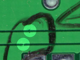
the etch was incomplete and left “short hairs” (my words) that are a pain to find. Each one is in a different place, some out in the open as in the image (and the easiest to find), while others were hidden under the silkscreening. You can also see a spot that has been over-etched. These errors all looked like a fiber had been laying across the board during etching.
The first few were discovered after I had built a couple Plague Bearers and found them working erratically. Then came the good old joy of troubleshooting! I’ve always had the approach of 1) Assume I screwed up or spaced out and forgot something, then 2) Verify components are good, and 3) Check the PCB. Which meant the errors took a while to find.
The short hairs are easy enough to fix once they’ve been found. Just a quick gouge with my homemade scraper/gouging tool and the boards were good to go. Now that I know what’s going on, I just check the boards with my continuity tester before assembly and fix the shorts. Not so simple with the Parasites.
As you can see in the picture, there is no pour due to component density. Therefore, these boards had the OPPOSITE problem: over-etching. It took me two boards and 14 hours a day for six days to find these bastards; they were all buried under silkscreening. The Parasite would work intermittently, flexing the board a little would make it stop working, or sometimes the unit would only work when warm – I found this one after I tested one, thought it good, and then went to bed. I checked it again in the morning and it didn’t work. What a mess.
Following all this, I’m forced to rescind the availability of the Parasites until I can get some reliable boards; these ones are just too much trouble to check. I’ll put some good news up in a few days, I’ve got a lot of catching up to do.
~flight
I was so excited to finally be using professionally-made PCBs. I spent a week researching the subject – how to make Gerber files, best layout practices (applied when possible, heh,) DRC (Design Rule Check) expectations and, most importantly, customer opinions.
I found this article to be quite helpful, and followed the links therein. After checking around I decided to go with Gold Phoenix. They had great reviews and are utilized by Sparkfun Electronics. I used the min/max tolerances stated here on Sparkfun’s BatchPCB site. The restrictions listed on the Gold Phoenix site are actually even closer tolerances, see #22 for “Outer Layer Line Width/Spacing”. I sent my order to Shane in Toronto, who was actually quite helpful and told me when my Gerbers were out of spec/missing dimensions. My Trace spacing was (accidentally – IMPORTANT NOTE TO EAGLE USERS: when you copy and paste your .brd file to make a large panel the DRCs do not tag along for the ride, you will need to re-enter them) 8mil for pours – tight, but in spec.
When the PCBs arrived – apparently, they had been delayed due to a holiday, the dangers of international commerce – I looked them over and thought they looked good. They had even made more than I had requested (as in the article on Near Future Laboratory.) Then I started building.
ABSOLUTE NIGHTMARE. So far, 60% of the Plague Bearer boards have been bad, and the two Parasite boards I attempted to build were bad as well. The types of anomalies varied as well. As you can see in this image:
the etch was incomplete and left “short hairs” (my words) that are a pain to find. Each one is in a different place, some out in the open as in the image (and the easiest to find), while others were hidden under the silkscreening. You can also see a spot that has been over-etched. These errors all looked like a fiber had been laying across the board during etching.
The first few were discovered after I had built a couple Plague Bearers and found them working erratically. Then came the good old joy of troubleshooting! I’ve always had the approach of 1) Assume I screwed up or spaced out and forgot something, then 2) Verify components are good, and 3) Check the PCB. Which meant the errors took a while to find.
The short hairs are easy enough to fix once they’ve been found. Just a quick gouge with my homemade scraper/gouging tool and the boards were good to go. Now that I know what’s going on, I just check the boards with my continuity tester before assembly and fix the shorts. Not so simple with the Parasites.
As you can see in the picture, there is no pour due to component density. Therefore, these boards had the OPPOSITE problem: over-etching. It took me two boards and 14 hours a day for six days to find these bastards; they were all buried under silkscreening. The Parasite would work intermittently, flexing the board a little would make it stop working, or sometimes the unit would only work when warm – I found this one after I tested one, thought it good, and then went to bed. I checked it again in the morning and it didn’t work. What a mess.
Following all this, I’m forced to rescind the availability of the Parasites until I can get some reliable boards; these ones are just too much trouble to check. I’ll put some good news up in a few days, I’ve got a lot of catching up to do.
~flight
posted by flight
at
3:57 PM
![]()
![]()
0 Comments :
Post a Comment
Links to this post :
Create a Link
<< Home